With almost 25 years of experience in the field of Non Destructive Testing and advanced imaging controls, INSIDIX provides a quick, reliable and precise expertise.
INSIDIX engineers have at their disposal :
- Acoustic microscopes (C-SAM)
- X Ray Radiography systems (2D)
- X Ray Laminography systems (3D)
- X Ray Tomography systems (3D-µCT)
- Lock in thermography systems (IR – LIT)
- Topography and Deformation measurement systems (TDM)
- X-Ray Micro-fluorescence system (XRF)
- Sample preparation systems (cutting, mounting, polishing)
- Scanning electron microscopy system (SEM)
- Optical microscope
- Manual Laser Scanner
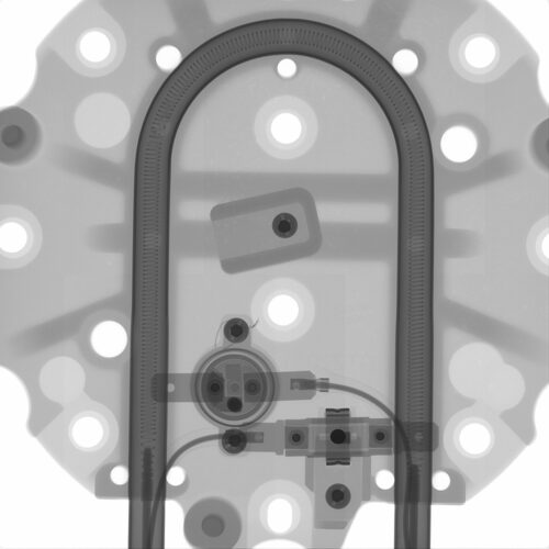
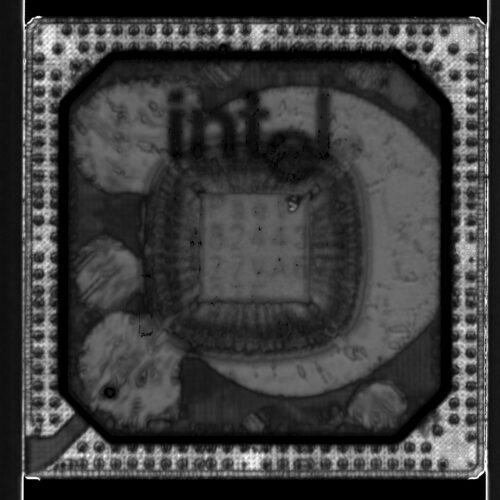
XRAY Radiography
Radiography is one of the oldest and most widely used methods of non-destructive testing. Radiography uses radiation energy to penetrate solid objects in order to assess variations in thickness or density, and for instance to detect cracks or other internal imperfections. The test object is placed between the radiation source and a digital detector. The image on the detector show the internal features of the test object.
Conventional 2D radiography is a shadowgraph of a 3D object, and information in depths and volume can be obtained observing the object with several orientations (angle).
Radiography can be used to inspect almost any material for defects, and can also be used to locate internal features, confirm the location of hidden parts in an assembly and to measure thickness of materials.
Applications :
- Fast production control
- Standards : IPC A610, Mil-Std883, Esa, ASTM, etc
- Parts sorting
- Brazing and solder pads quality (porosity, surface rate)
- Inspection of solder joints for electronic components through and SMT (BGA, QFN, QFP, capacitors, resistance, coils…)
- Contacts (on/off), connectors
- Check design & assembly
- Inclusions, heterogeneities, porosities, cracks in material (eg. ceramic)
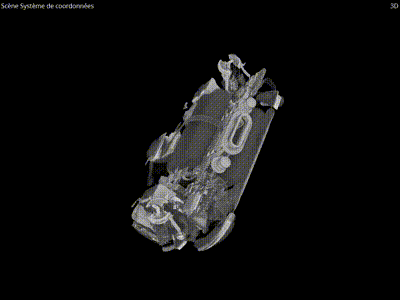
3D XRAY Computed Tomography
Scanning Electron Microscopy
A scanning electron microscope (SEM) is a type of electron microscope that produces images of a sample by scanning the surface with a focused beam of electrons. The electrons interact with atoms in the sample, producing various signals that contain information about the surface topography and composition of the sample.
These microscopes are used in nanotechnologies, material sciences, failure analyses, semiconductors or even biology.
Our SEM is equipped with Energy-dispersive X-ray spectroscopy (EDS) for chemical characterization/elemental analysis of materials.
INSIDIX has also a state of the art preparation lab that allows optimum surface quality for inspection.
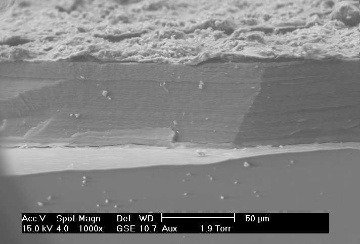
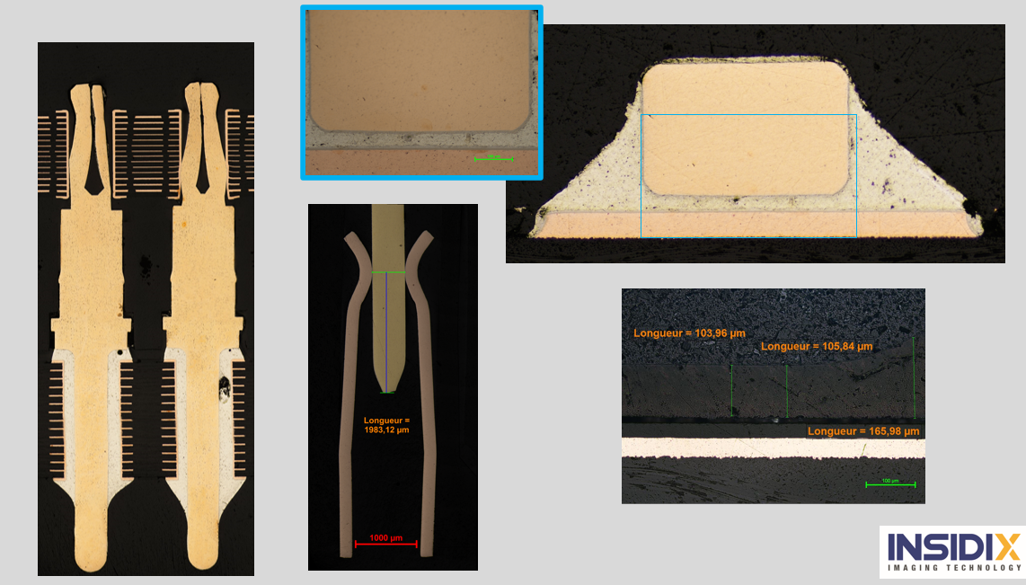
Metallography
INSIDIX proposes metallographic cross section analysis for defect detection .
Cutting
The first step is usually to isolate the region of interest on the part to analyse. This is done using a cutting equipment design for precise and quick cut of any sample.
Mounting
The cut part is then mounted using specific resin (Epoxy or thermoplastics). The use of this technic stiffens the part, to make it compatible with the next step of the preparation.
Polishing
Finally, the mounted tablet is polished up until the desired section plane. The polishing is made using several abrasive papers, to get an optimal surface quality.
Use of optical microscope and evaluation
The inspection of the section plane is done using an optical microscope (or a SEM).
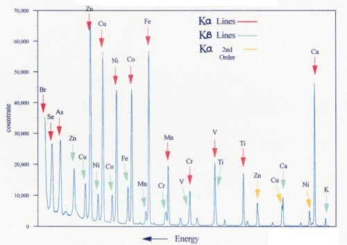
X-ray fluorescence
X-ray fluorescence (XRF) is the emission of characteristic “secondary” (or fluorescent) X-rays from a material that has been excited by being bombarded with high-energy X-rays or gamma rays. The phenomenon is widely used for elemental analysis and chemical analysis, particularly in the investigation of metals, glass, ceramics and building materials, and for research in geochemistry, forensic science, archaeology and art objects.
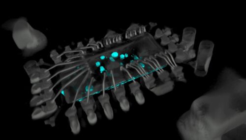
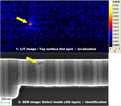
Lock-In Thermography - LIT
Infrared thermography can assist in understanding material heterogeneities, characterize heat dissipation or spreading, or electrical failures localization (short circuit or leakage).
Analyses done under thermal, electrical, magnetic (RFID) load.
With Dynamic or lock-in Infrared Thermography (LIT),sensitivity is increased and « hot spot » of some 10-3 °C are detected. Heat dissipation: observation of a full board or system, temperature mapping and measurement, visualization of hot components or areas. Comparison with spec. or models
– Leakage and Short-circuit source (incl. CAF) localization, very fast and accurate (up to 6µm): in only few hours a hot spot is detected and allows to guaranty defect finding ( current compliance ensure no burning , localization data are transmitted for deprocessing ).
Applications :
- Fast localization of leakage, short-circuit
- Heat spreading efficiency, heat dissipation
- Thermal homogeneity
- Check specification, check design, or model
- Sealing joints
- Brazed and welded joints
- Qualification and fast selection of glues, adhesive, comparative analyses of aging, etc
- Inclusions, heterogeneities, porosities, cracks in material
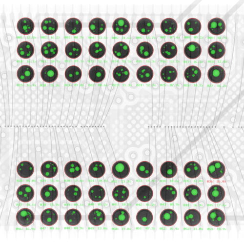
Scannig accoustic microscopy
Acoustic microscopy (SAM) is a non-invasive & non-destructive technique that can be used to image the internal features of a specimen, in particular its interfaces. SAM is a superior tool to detect delaminations even of sub-micron thicknesses (down to 100nm !). SAM is particularly useful for inspection of small or complex optical devices, electronic devices. SAM can also be used to measure the thickness of an internal layer of material. Overall, SAM is an efficient tool for evaluating sealing quality, printed circuit boards, underfills, BGA, QFN, passive components, and wafers.
SAM systems use sound energy to image a sample through the use of transducers. Samples are submerged in a liquid medium to ensure the ultrasound waves propagate to and through the samples. The ultrasonic transducers send pulses into the liquid. The transducer also receives reflected pulses (echoes) from discontinuities and disturbances from the sample. The transducer transforms the reflected sound pulses into electromagnetic pulses which are displayed as pixels with defined gray values thereby creating an image.
A complementary imaging technology is acoustic Tomographiy (SALI). It allows to slice a sample into as many as 100 images using a single scan. The image data set allows to investigate different interfaces.
Applications :
- Fast production control
- Standards : IPC A610, Mil-Std883, J-Std-035, Esa, etc
- Parts sorting
- Inspection of solder pads, flip-chip, underfill, die-attach
- Sealing joints
- Brazed and welded joints
- Qualification and fast selection of glues, adhesive, comparative analyses of aging, etc
- Inclusions, heterogeneities, porosities, cracks in material
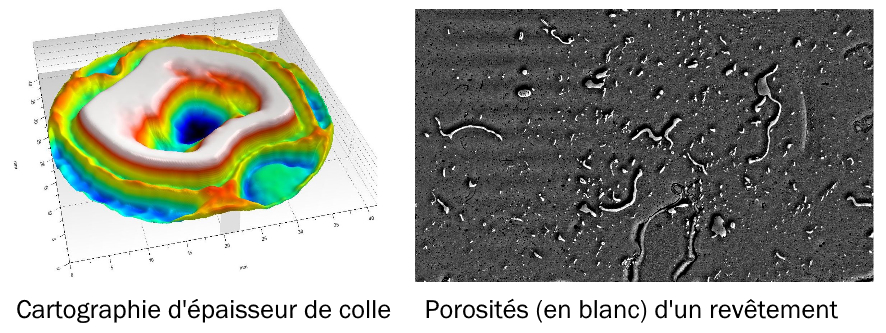
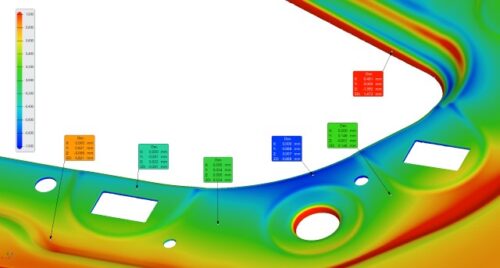
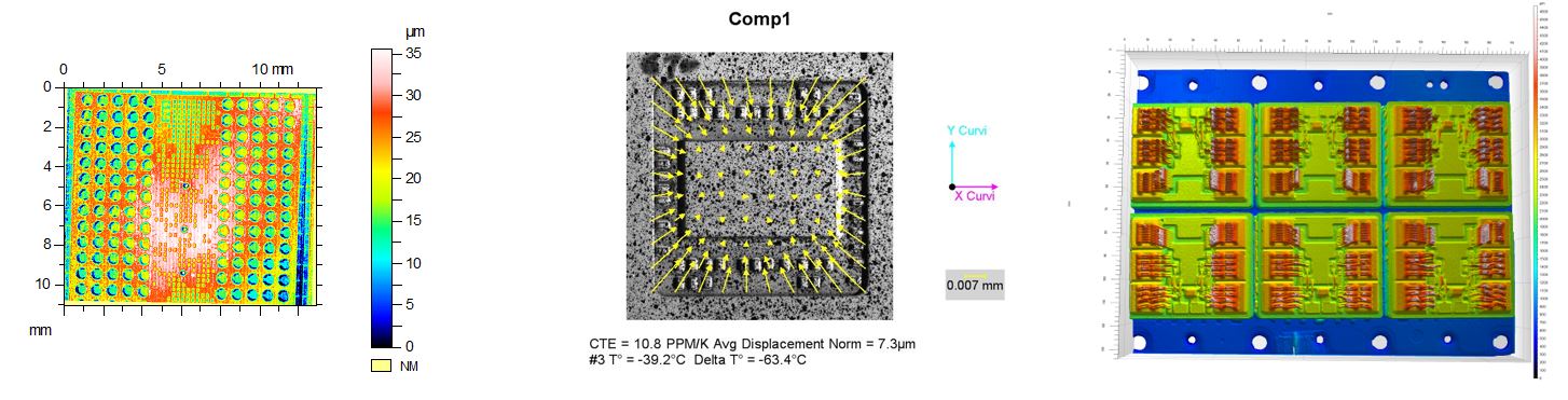
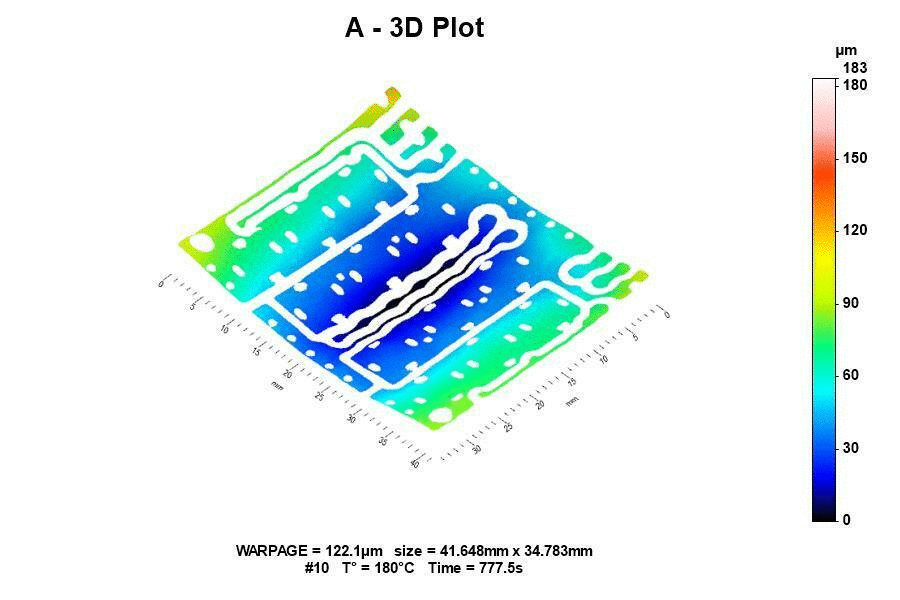
Topography and deformation measurement
Check: www.tdm-3D.com
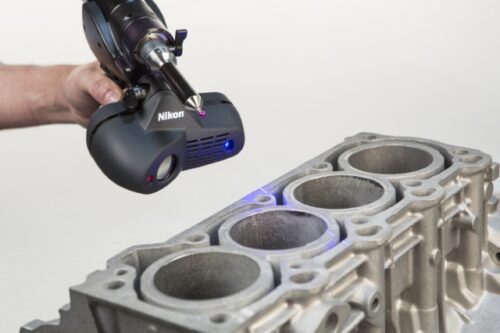
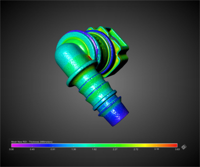
Manual Laser Scanning
Nikon’s premium ModelMaker H120 laser scanner and MCAx S 7-axis articulated portable CMM arm form a leading-edge 3D measurement solution, enabling users to accelerate time to market and streamline manufacturing processes.
Key elements :
Class-Leading Handheld Scanning
ModelMaker H120 rapidly measures almost any size of part or surface finish, capturing small details at class-leading accuracy in any industrial environment.
Precision Portable Measurement
The accuracy, ease-of-use and flexibility of the 7-axis MCAx S arm delivers fast and precise probing as well as scanning, even when operating wirelessly.
Proven System Performance
For total confidence in the solution, every delivered combination of ModelMaker H120 and MCAx S receives ISO 10360-8:2013 Annex D system scanning performance certification.